Welcome to visit the website of HJ Polymer China Co., Ltd. ---Semi-conductive Compound Industry Solutions


 中文简体
中文简体 Français
 عربى
عربى

Welcome to visit the website of HJ Polymer China Co., Ltd. ---Semi-conductive Compound Industry Solutions

Content
In a medium or high voltage power cable, the semiconductive shield layer is only a fraction of a millimetre thick, yet it carries an outsized share of the cable's long-term reliability. It smooths the electric field around the conductor, fills the gaps between strands, and protects the insulation from the sharp edges and voids that would otherwise become partial discharge sites. A shield layer that looks acceptable on the reel can still hide defects that only surface after years in service.
We have been manufacturing semiconductive shielding compounds since 2002, and the defect reports cable makers bring to us tend to repeat. The seven below are the ones we encounter most often, together with the root causes behind them.
A semiconductive shield is a carbon black filled polymer, co-extruded in three layers with the insulation and the other shield. Because the layer is thin and the interface area is enormous, small disturbances have nowhere to hide. A protrusion of a few tens of microns, a single void, or a patch of poorly dispersed carbon black can locally distort the electric field and start the degradation process that ends in a failure.
When we investigate a complaint, the root cause almost always sits in one of three places: the compound itself, the extrusion line, or the handling that follows. Sorting the visible symptom into one of the seven patterns below usually tells you which of the three to examine first.
| Defect | Where it usually appears | Most common root cause family |
|---|---|---|
| Protrusions and surface roughness | Bonded interface between shield and insulation | Filtration, die condition, temperature profile |
| Microvoids and gas bubbles | Inside the shield layer, often near the conductor | Moisture and volatiles, vacuum, melt pressure |
| Bond strength too high or too low | Insulation shield during stripping | Formulation, cooling rate, line speed |
| Thickness variation and eccentricity | Along the length and around the circumference | Tooling concentricity, output fluctuation |
| Gels, fisheyes and contamination | Random spots through the layer | Purge discipline, handling, screen condition |
| Carbon black agglomerates | Conductor shield, resistivity checks | Mixing and compounding, feeding, screening |
| Scorch, pre-cure and moisture marks | Shield surface and cross-section | Residence time, cooling water, storage |
Protrusions are raised points on the shield surface that push into the insulation. They are counted per unit area on microtome slices, and the count grows quickly when the process drifts.
Root causes we see most often:
Voids are the classic electrical weak point: they distort the field, ignite partial discharge, and feed water treeing. They show up in slice inspections as small round cavities, often clustered near the conductor.
Root causes:
Bond strength between the insulation shield and the insulation is a narrow window. Too tight, and the installer cannot strip the cable cleanly without nicking the insulation. Too loose, and the interface can open up, letting moisture travel along the cable. Both extremes are usually reported as one defect: the shield does not strip properly.
Root causes:
For medium voltage cables, a strippable grade does much of this work at the formulation stage rather than on the line. HJ0602 is built around exactly that balance.
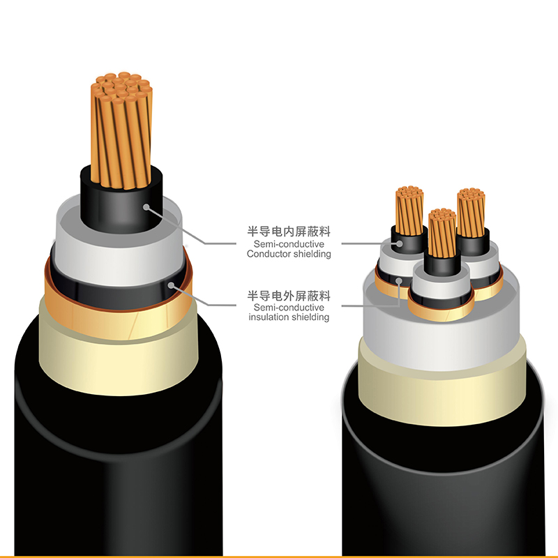 HJ0602 Easy-Strippable Insulation Shielding Compound for MV Power CablesEasy-strippable insulation shield for MV cables up to 36 kV, with low peel force and stable extrusion, useful where uniform shielding and clean separation matter.View Product →
An uneven shield thickness is a quiet defect. It rarely fails immediately, but the thin side loses its stress-grading margin while the thick side wastes material and may bond differently.
Root causes:
These appear as discrete spots with a different colour or texture. Under the microscope they are clearly foreign to the compound: crosslinked gel, dust, fibre, or a piece of degraded material.
Root causes:
A shield that conducts unevenly is worse than one that conducts poorly. Agglomerates raise local resistivity enough to create hot spots and uneven stress grading, and they can also disturb adhesion at the interface.
Root causes:
This is one area where compound quality decides the outcome before the cable maker touches a setting. A conductor shield such as HJ0301 is built around dispersion and screening that keep agglomerates out of the pellet.
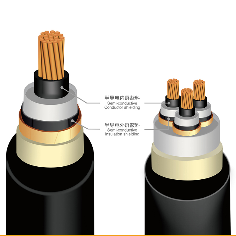 HJ0301 Semi-Conductive Conductor Shielding Compound for MV Power CablesBonded conductor shielding compound for MV cables up to 36 kV, designed to resist scorch and copper oxidation while supporting stable, clean extrusion.View Product →
Scorch appears as hard, partially crosslinked particles or as a rough, matt surface. Marks left by water droplets look cosmetic, but they often sit on top of a locally rough interface.
Root causes:
When a defect appears, the most useful first step is not to change a setting but to characterise the symptom properly. Measure the defect size, count it per unit area, and note where it sits: at the start of a run or in steady state, on the conductor shield or the insulation shield, evenly distributed or clustered. Each observation removes whole branches from the fault tree.
From there, work through three checks in order. First, material history: lot number, storage conditions, moisture content, and how the bags were handled. Second, machine condition: temperatures, vacuum, screen condition, purge records, and tooling wear. Third, the interface itself: slice the cable and look at what the shield is actually touching. Only after that is it worth adjusting the process, because random changes destroy the evidence you need.
A compound supplier who understands the extrusion line can shorten this loop considerably. Our power cable shield compounds cover conductor shields, insulation shields, and bonded or strippable systems across voltage levels, and the technical discussion usually starts with the defect pattern rather than the datasheet. For high voltage work, HJ0901 combines conductor and insulation shielding functions in one grade.
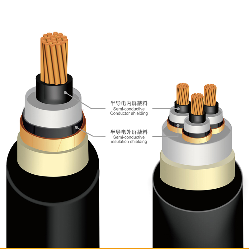 HJ0901 Conductor and Insulation Shielding Compound for HV CablesFor high-voltage cables up to 132 kV, this ultra-clean, super-smooth grade combines conductor and insulation shielding in one compound.View Product →
To go deeper into how compound composition and performance interact with processing, our technical note on semiconductive compound composition and selection walks through the same variables from the material side.
Seven defects, but the same short list of root causes keeps reappearing: moisture, temperature, contamination, and tooling. None of them is exotic, and none is solved by a single setting. What makes the difference is a shared vocabulary between the cable maker and the compound supplier, so that a symptom at the interface points quickly to the process step or material variable responsible.
If you are working through a shield layer problem right now, send us your slice photos and run data. That is usually enough for us to tell you whether the cause sits in the compound, the line, or the handling after the tube.
![HJ0901 Semi-conductive Conductor and Insulation Shielding Compound for HV Power Cables [Super Clean and Smooth]](/hjcheme/2026/02/04/5-zhjG.jpg "HJ0901 Semi-conductive Conductor and Insulation Shielding Compound for HV Power Cables [Super Clean and Smooth]")
![HJ0602 Semi-conductive Insulation Shielding Compound For MV Power Cables [Easy Strippable Grade]](/hjcheme/2026/01/30/5-EN1N.jpg "HJ0602 Semi-conductive Insulation Shielding Compound For MV Power Cables [Easy Strippable Grade]")
![HJ0605 Semi-conductive Insulation Shielding Compound for MV Power Cables [Copper Oxidation Resistance Grade]](/hjcheme/2026/02/04/2-tK2C.jpg "HJ0605 Semi-conductive Insulation Shielding Compound for MV Power Cables [Copper Oxidation Resistance Grade]")
![HJ0604 Semi-conductive Insulation Shielding Compound for MV Power Cables [Fast Line Speed Grade]](/hjcheme/2026/02/04/1.jpg "HJ0604 Semi-conductive Insulation Shielding Compound for MV Power Cables [Fast Line Speed Grade]")
![HJ0603 Semi-conductive lnsulation Shielding Compound for MV Power Cables [Super Clean Grade]](/hjcheme/2026/01/30/1-h8nu.jpg "HJ0603 Semi-conductive lnsulation Shielding Compound for MV Power Cables [Super Clean Grade]")



