Welcome to visit the website of HJ Polymer China Co., Ltd. ---Semi-conductive Compound Industry Solutions


 中文简体
中文简体 Français
 عربى
عربى

Welcome to visit the website of HJ Polymer China Co., Ltd. ---Semi-conductive Compound Industry Solutions

Content
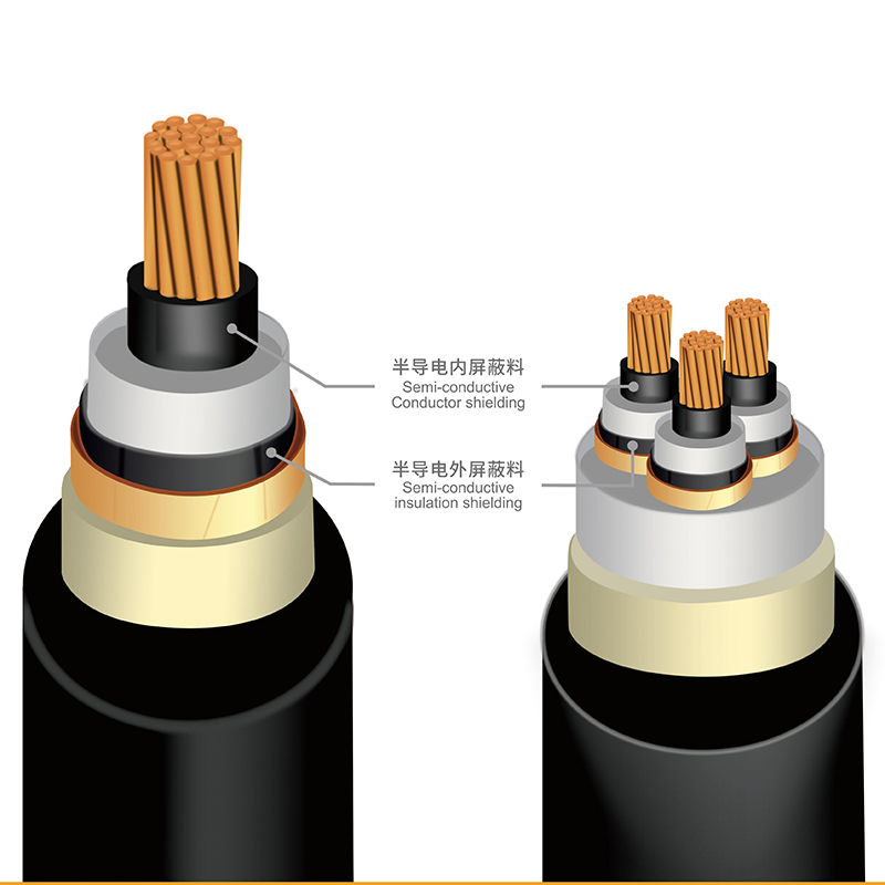
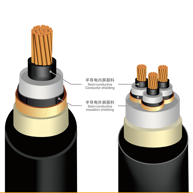
Cut open a medium- or high-voltage power cable and you'll find two thin black layers sandwiching the insulation: one wrapped directly around the conductor, the other applied over the insulation before the metallic shield. Both are made from semi-conductive compound, and both are co-extruded with the insulation in a single pass through the extrusion line.
Neither layer carries current in the conventional sense. Their job is geometric and electrical rather than functional in the way the conductor or insulation is. The conductor shield smooths out the irregular surface created by stranded copper or aluminum wires, while the insulation shield does the same at the outer boundary, creating a clean, continuous transition into the grounded shield layer.
This positioning matters because the interface between semi-conductive and insulating layers is where electrical stress concentrates most in an operating cable. Any irregularity at that interface becomes a starting point for degradation, which is why the compound's properties are specified almost as tightly as the insulation itself.
An uncoated conductor made of twisted strands presents a bumpy, non-uniform surface to the electric field. Voltage stress doesn't distribute evenly across a bumpy surface — it concentrates at the high points, the same way water pressure concentrates at the tip of a sharp object. Left unmanaged, those concentration points become sites for partial discharge, a form of localized electrical breakdown that erodes insulation from the inside over months or years.
Semi-conductive compound solves this by creating an isopotential surface: a boundary where voltage stays uniform regardless of what lies beneath it. A well-formulated compound with proper carbon black dispersion eliminates the sharp gradients that would otherwise form at each strand or surface defect.
The consequences of getting this wrong aren't cosmetic. A cable with a rough or poorly dispersed semi-conductive layer may pass initial electrical testing and still fail years into service, once repeated thermal cycling and voltage stress have had time to work on hidden imperfections. This is one reason cable manufacturers treat semi-conductive compound quality control as seriously as insulation quality control, even though the material itself carries no rated voltage.
A typical semi-conductive compound for MV or HV cable combines three functional components. The base resin is usually an ethylene copolymer — ethylene-butyl acrylate, ethylene-ethyl acrylate, or ethylene vinyl acetate are common choices, selected for their compatibility with the polar surface chemistry of carbon black and their ability to bond well with adjacent insulation during co-extrusion.
Carbon black is the conductive filler, typically loaded at 30 to 70 parts per hundred parts of resin. Two grades dominate: acetylene black and furnace black, chosen for high structure and controlled surface area, generally in the 60–150 m²/g range. Ash content matters more than most buyers realize — even trace mineral contamination in the carbon black can create localized weak points in the finished layer.
Rounding out the formulation are cross-linking agents (usually peroxides), cross-linking inhibitors to control scorch behavior during processing, antioxidants for long-term thermal stability, and processing aids such as fatty acid esters that improve carbon black dispersion and extrudate surface finish. Each of these plays a narrow but essential role — remove the inhibitor and the compound may cure prematurely inside the extruder; skip the dispersion aid and surface smoothness suffers even with good raw carbon black.
Surface smoothness is measured directly: industry practice caps the number of protrusions between 50 and 100 micrometers at roughly five per square centimeter or fewer. This isn't an arbitrary aesthetic standard — protrusions of that size are large enough to create the field concentrations discussed earlier.
Volume resistivity determines how effectively the layer performs its stress-grading function; compounds that drift toward the insulating end of the spectrum defeat the purpose of the layer entirely. Scorch time, tested according to ASTM D1646 and typically expected to exceed forty minutes at 145°C, tells a compounder and cable manufacturer how much processing latitude they have before premature cross-linking becomes a risk on the line.
Melt index, usually specified in the 1 to 30 g/10 min range at 190°C and 2.16 kg, governs how the compound flows during extrusion and how well it co-extrudes with the insulation layer at matched viscosities. A mismatch here shows up as an uneven interface even when both individual materials meet their own specifications in isolation.
| Property | Typical Target | Why It Matters |
|---|---|---|
| Surface protrusions (50–100 μm) | ≤ 5 per cm² | Prevents local field concentration |
| Scorch time at 145°C | ≥ 40 minutes | Processing safety margin |
| Melt index (190°C, 2.16 kg) | 1–30 g/10 min | Co-extrusion compatibility |
| Carbon black surface area | 60–150 m²/g | Balances conductivity and dispersion |
Voltage class drives formulation choices more than any other single factor. Low-voltage cable can tolerate looser tolerances on surface smoothness and resistivity because stress levels are modest. Move into medium-voltage territory and specifications tighten noticeably; by the time you're formulating for high-voltage or ultra-high-voltage direct current transmission, even a small increase in rated voltage forces a disproportionate improvement in shield quality — roughly a fifty-fold jump in voltage may only permit the semi-conductive layer thickness to double, meaning the material itself has to do more of the work.
Process compatibility is the second axis. Traditional peroxide-cross-linked systems built on ethylene copolymers remain the dominant approach for XLPE-insulated cable, but polypropylene-based semi-conductive screens have gained ground alongside PP insulation systems (PP-TPE, PP-TPO, HPTE), offering better recyclability and, in some formulations, elimination of the peroxide cure step entirely. Choosing between these isn't purely a performance question — it also depends on what insulation system the compound needs to co-extrude with and what curing infrastructure the manufacturing line already has.
For buyers comparing suppliers, it helps to request scorch time and melt index data measured under conditions matching your actual line speed and temperature profile, not just standard test conditions. A compound that looks identical on a datasheet can behave differently once it's running through equipment operating outside the test lab's assumptions.
Most semi-conductive compound failures trace back to one of three root causes. Poor carbon black dispersion is the most frequent: even correctly specified carbon black will produce a rough, defect-prone surface if it isn't distributed evenly through the resin matrix during compounding. This is largely a mixing equipment and process control issue rather than a raw material one, which is why compounders increasingly rely on specialized co-kneading equipment designed specifically for high-filler-loading conductive compounds.
Ash content contamination is the second common issue. Carbon black with elevated ash content introduces mineral impurities that create localized weak points, and these defects are often invisible until the cable is under load and thermal cycling has had time to reveal them.
Premature cross-linking, or scorch, is the third. If a compound's scorch time is too short for the actual extrusion conditions on a given line, partial curing inside the extruder produces gel particles that show up as visible defects in the finished layer. The fix is rarely a different compound altogether — it's usually a closer match between the compound's scorch characteristics and the specific line's residence time and temperature profile, which is exactly why datasheet values should be treated as a starting point for line trials rather than a guarantee of in-service performance.
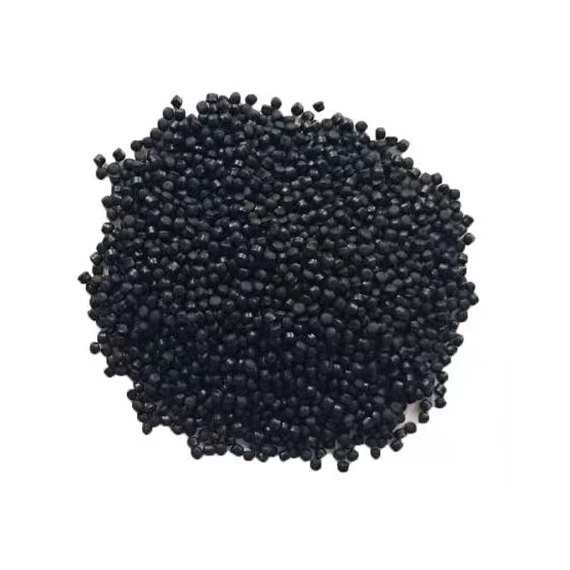
![HJ0901 Semi-conductive Conductor and Insulation Shielding Compound for HV Power Cables [Super Clean and Smooth]](/hjcheme/2026/02/04/5-zhjG.jpg "HJ0901 Semi-conductive Conductor and Insulation Shielding Compound for HV Power Cables [Super Clean and Smooth]")
![HJ0302 Semi-conductive Insulation And Conductor Shielding Compound for MV Power Cables [Bonded Insulation Grade]](/hjcheme/2026/01/30/1-oGlm.jpg "HJ0302 Semi-conductive Insulation And Conductor Shielding Compound for MV Power Cables [Bonded Insulation Grade]")
![HJ0305 Semi-conductive Conductor Shielding Compound for MV Power Cables [Copper oxidation resistance Grade]](/hjcheme/2026/01/30/2-ybjb.jpg "HJ0305 Semi-conductive Conductor Shielding Compound for MV Power Cables [Copper oxidation resistance Grade]")