Welcome to visit the website of HJ Polymer China Co., Ltd. ---Semi-conductive Compound Industry Solutions


 中文简体
 Français
 عربى


Welcome to visit the website of HJ Polymer China Co., Ltd. ---Semi-conductive Compound Industry Solutions

Content
Walk along a semicon extrusion line for a few minutes and you can usually sense whether the compound in the hopper is behaving. The head pressure is steady, the surface is glass-smooth, the screen pack is not climbing. When something drifts, the conversation almost always comes back to one ingredient: carbon black.
Carbon black is a modest share of a semiconductive compound by cost, yet it decides whether a shielding layer conducts properly, extrudes cleanly and stays reliable for decades in service. Among all the variables we deal with, two are consistently underestimated — the grade of carbon black selected, and the quality of its dispersion in the polymer. Having compounded cable shielding materials since 2002, we have seen both make the difference between a comfortable run and a week of firefighting.
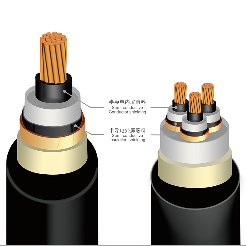
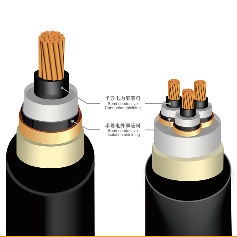
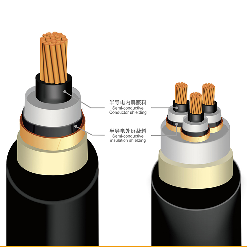
A semiconductive shield sits between the metal conductor or the insulation and the outside world. It is not a conductor and it is not an insulator; it is a carefully tuned middle ground, typically specified in tens to a few hundred ohm-centimetres depending on voltage class and the standard being applied. That narrow window exists because the shield must grade the electric field and hold the insulation surface at a uniform potential, without introducing losses of its own.
The polymer matrix — crosslinked polyethylene, EVA, EPR or a blend — is essentially an insulator. Conductivity comes entirely from the carbon black network that forms once the loading passes the percolation threshold. In practice, semiconductive compounds carry roughly 25 to 40 percent carbon black by weight. Below the threshold, resistivity is unpredictable and temperature-sensitive; far above it, viscosity climbs, surface quality suffers, and the extra loading buys nothing except cost and processing trouble.
So the network is the product. Whether that network is continuous, uniform and stable depends on the intrinsic properties of the black and on how completely it has been broken down and distributed.
Carbon black is not a commodity that can be swapped by weight. Two grades at identical loading can differ by orders of magnitude in resistivity and by a visible margin in surface finish. The table below summarises the parameters we track when a grade is evaluated for semiconductive use.
| Parameter | What it influences | What to watch |
|---|---|---|
| Primary particle and aggregate size | Number of conductive contact points, percolation threshold, surface smoothness | Finer grades conduct at lower loading but demand more mixing energy |
| Structure (DBP absorption) | Network formation, conductivity at a given loading, compound viscosity | Higher structure eases conductivity but raises torque and die pressure |
| Surface area (BET or iodine adsorption) | Polymer wetting, viscosity, tendency to adsorb volatiles | High-surface-area grades need careful feeding and tighter dispersion control |
| Volatile content and pH | Degassing behaviour, interaction with the crosslinking system, void formation | Low volatiles are preferred for high-voltage layers; consistency matters as much as the value |
| Ash, sulphur and ionic impurities | Dielectric losses, cleanliness, long-term aging behaviour | Apply tight limits for high-voltage work and keep full lot traceability |
| Grit and contamination | Screen pack pressure, protrusions, surface defects | Set filtration limits and verify them with pressure filtration testing |
If there is one trade-off worth internalising, it is this: conductivity is easy to buy, and difficult to buy cleanly. A high-structure, high-surface-area black will build a conductive network at lower loading and give generous electrical margins. It will also raise compound viscosity, increase mixing torque, generate more heat and make every downstream step less forgiving.
A finer, lower-structure grade can deliver excellent surface smoothness at the interface — exactly what high-field applications want — but it resists wetting and needs real dispersion energy to reach its potential. Choose it without the mixing capability to match and you end up with a compound that looks fine on paper and underperforms on the line.
The right window therefore depends on voltage class, insulation interface requirements, the process in use (Sioplas, single-step, fast lines) and the extrusion equipment downstream. There is no universally best grade, only a grade that fits a defined duty.
A good grade is a necessary condition, not a sufficient one. Carbon black arrives as agglomerates far larger than the primary particles, and those agglomerates must be broken down and distributed evenly through the melt. Any that survive become local insulating islands: resistivity turns non-uniform, current crowds around them, and the field distribution in service is no longer what the design assumed.
The effects compound. Undispersed particles create protrusions at the semicon–insulation interface, and protrusions concentrate electric stress in exactly the place where the insulation can least afford it. Poor dispersion also encourages space charge accumulation, weakens interfacial bonding where a bonded shield is required, and scatters surface roughness readings that would otherwise pass.
On the line, the symptoms are just as concrete: rising screen pack pressure, more frequent screen changes, occasional surface defects, and batch-to-batch variation in head pressure that operators learn to compensate for instead of solving. All of it traces back to mixing energy, feeding strategy and residence time distribution.
No single test tells the whole story, so we look at several together and compare them against the compound's duty:
For a broader view of how composition, performance and selection criteria fit together, our technical note on semiconductive compound composition and selection goes into more detail.
High-voltage layers are the strictest case. Ash and ionic impurity limits tighten, volatile content must be low for degassing, and dispersion has to be near-complete because the field is unforgiving. Cleaner, finer blacks with tight lot control are the starting point; ultraclean compounding and filtration do the rest.
 HJ0901 High-Voltage Semi-Conductive Shielding CompoundFor high-voltage cable conductor and insulation shielding up to 132 kV, offering ultra-clean surfaces, stable resistivity and dry-vulcanization processing.View Product →
Medium-voltage work spreads across a wider range of requirements. Conductor shields face a rougher surface and different bonding demands, while insulation shields must balance smoothness, strippability and adhesion depending on the cable design. Here the grade choice is often about matching the black to the stripping behaviour and the line speed rather than chasing the lowest possible resistivity.
 HJ0301 Medium-Voltage Conductor Shielding CompoundDesigned for bonded conductor shielding in medium-voltage cables up to 36 kV, with good extrusion flow, thermal stability and copper-interface protection.View Product →
 HJ0601 Strippable Medium-Voltage Insulation Shielding CompoundFor insulation shielding in medium-voltage cables up to 36 kV, combining good strippability, smooth extrusion and stable volume resistivity for high-speed lines.View Product →
Low- and medium-voltage thermoplastic systems used with Sioplas processing add a further constraint: the compound must develop its network without crosslinking, so dispersion quality has to be delivered in the melt rather than rescued later. The full range is set out under our power cable shield compounds.
When a customer asks which grade to use, the honest answer usually starts with questions about the cable, not the carbon black. Voltage class, insulation interface, extrusion line, stripping requirement, and the standard the finished cable is tested against all narrow the field before a single grade is shortlisted.
From there, we prefer to specify the grade and the dispersion together, as one target rather than two. A grade specification without a dispersion specification invites variation; a dispersion specification without the right grade simply polishes the wrong material. Incoming carbon black inspection, mixing parameter windows, filtration limits and finished-compound release tests should all point at the same property: a uniform, stable, clean conductive network.
That is also why lot-to-lot consistency deserves as much attention as any headline number. A compound that performs beautifully on one shipment of black and drifts on the next is not a specification — it is a coincidence.


